- 您现在的位置:买卖IC网 > Sheet目录329 > IDT70V37L20PFI (IDT, Integrated Device Technology Inc)IC SRAM 576KBIT 20NS 100TQFP
IDT70V37L
High-Speed 3.3V 32K x 18 Dual-Port Static RAM
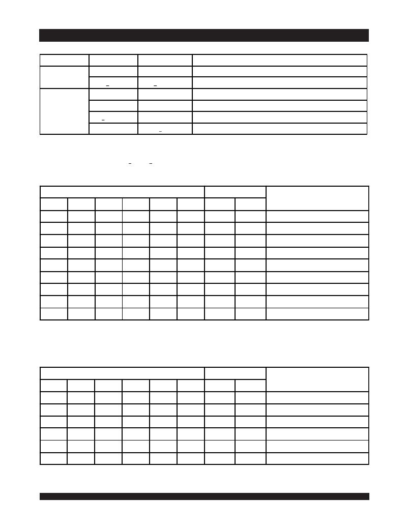
Truth Table I – Chip Enable (1,2)
Industrial and Commercial Temperature Ranges
X
NOTES:
CE
L
H
CE 0
V IL
< 0.2V
V IH
X
>V DD -0.2V
X (3)
CE 1
V IH
>V DD -0.2V
X
V IL
(3)
<0.2V
Port Selected (TTL Active)
Port Selected (CMOS Active)
Port Deselected (TTL Inactive)
Port Deselected (TTL Inactive)
Port Deselected (CMOS Inactive)
Port Deselected (CMOS Inactive)
Mode
4852 tbl 06
1. Chip Enable references are shown above with the actual CE 0 and CE 1 levels; CE is a reference only.
2. 'H' = V IH and 'L' = V IL .
3. CMOS standby requires 'X' to be either < 0.2V or >V DD -0.2V.
Truth Table II – Non-Contention Read/Write Control
Inputs (1)
Outputs
CE (2)
H
X
L
L
L
L
L
L
X
R/ W
X
X
L
L
L
H
H
H
X
OE
X
X
X
X
X
L
L
L
H
UB
X
H
L
H
L
L
H
L
X
LB
X
H
H
L
L
H
L
L
X
SEM
H
H
H
H
H
H
H
H
X
I/O 9-17
High-Z
High-Z
DATA IN
High-Z
DATA IN
DATA OUT
High-Z
DATA OUT
High-Z
I/O 0-8
High-Z
High-Z
High-Z
DATA IN
DATA IN
High-Z
DATA OUT
DATA OUT
High-Z
Mode
Deselected: Power-Down
Both Bytes Deselected
Write to Upper Byte Only
Write to Lower Byte Only
Write to Both Bytes
Read Upper Byte Only
Read Lower Byte Only
Read Both Bytes
Outputs Disabled
NOTES:
1. A 0L — A 14L ≠ A 0R — A 14R
2. Refer to Truth Table I - Chip Enable.
Truth Table III – Semaphore Read/Write Control (1)
4851 tbl 07
Inputs (1)
Outputs
CE (2)
H
X
H
X
L
L
R/ W
H
H
↑
↑
X
X
OE
L
L
X
X
X
X
UB
X
H
X
H
L
X
LB
X
H
X
H
X
L
SEM
L
L
L
L
L
L
I/O 9-17
DATA OUT
DATA OUT
DATA IN
DATA IN
______
______
I/O 0-8
DATA OUT
DATA OUT
DATA IN
DATA IN
______
______
Mode
Read Data in Semaphore Flag
Read Data in Semaphore Flag
Write I/O 0 into Semaphore Flag
Write I/O 0 into Semaphore Flag
Not Allowed
Not Allowed
NOTES:
1. There are eight semaphore flags written to I/O 0 and read from all the I/Os (I/O 0 -I/O 17 ). These eight semaphore flags are addressed by A 0 -A 2 .
2. Refer to Truth Table I - Chip Enable .
6.42
4851 tbl 08
发布紧急采购,3分钟左右您将得到回复。
相关PDF资料
IDT70V38L15PFG
IC SRAM 1.125MBIT 15NS 100TQFP
IDT70V525ML55BZI
IC SRAM 128KBIT 55NS 144FBGA
IDT70V5388S166BGI
IC SRAM 1.125MBIT 166MHZ 272BGA
IDT70V631S10PRFG
IC SRAM 4MBIT 10NS 128TQFP
IDT70V639S12PRFI
IC SRAM 2.25MBIT 12NS 128TQFP
IDT70V659S12DRI
IC SRAM 4MBIT 12NS 208QFP
IDT70V7319S166BCI
IC SRAM 4MBIT 166MHZ 256BGA
IDT70V7339S166BCI
IC SRAM 9MBIT 166MHZ 256BGA
相关代理商/技术参数
IDT70V37L20PFI8
功能描述:IC SRAM 576KBIT 20NS 100TQFP RoHS:否 类别:集成电路 (IC) >> 存储器 系列:- 标准包装:1,000 系列:- 格式 - 存储器:RAM 存储器类型:SRAM - 双端口,同步 存储容量:1.125M(32K x 36) 速度:5ns 接口:并联 电源电压:3.15 V ~ 3.45 V 工作温度:-40°C ~ 85°C 封装/外壳:256-LBGA 供应商设备封装:256-CABGA(17x17) 包装:带卷 (TR) 其它名称:70V3579S5BCI8
IDT70V38L15PF
功能描述:IC SRAM 1.125MBIT 15NS 100TQFP RoHS:否 类别:集成电路 (IC) >> 存储器 系列:- 标准包装:3,000 系列:- 格式 - 存储器:EEPROMs - 串行 存储器类型:EEPROM 存储容量:8K (1K x 8) 速度:400kHz 接口:I²C,2 线串口 电源电压:1.7 V ~ 5.5 V 工作温度:-40°C ~ 85°C 封装/外壳:8-SOIC(0.154",3.90mm 宽) 供应商设备封装:8-SOIC 包装:带卷 (TR)
IDT70V38L15PF8
功能描述:IC SRAM 1.125MBIT 15NS 100TQFP RoHS:否 类别:集成电路 (IC) >> 存储器 系列:- 标准包装:1,000 系列:- 格式 - 存储器:RAM 存储器类型:SRAM - 双端口,同步 存储容量:1.125M(32K x 36) 速度:5ns 接口:并联 电源电压:3.15 V ~ 3.45 V 工作温度:-40°C ~ 85°C 封装/外壳:256-LBGA 供应商设备封装:256-CABGA(17x17) 包装:带卷 (TR) 其它名称:70V3579S5BCI8
IDT70V38L15PFG
功能描述:IC SRAM 1.125MBIT 15NS 100TQFP RoHS:是 类别:集成电路 (IC) >> 存储器 系列:- 标准包装:3,000 系列:- 格式 - 存储器:EEPROMs - 串行 存储器类型:EEPROM 存储容量:8K (1K x 8) 速度:400kHz 接口:I²C,2 线串口 电源电压:1.7 V ~ 5.5 V 工作温度:-40°C ~ 85°C 封装/外壳:8-SOIC(0.154",3.90mm 宽) 供应商设备封装:8-SOIC 包装:带卷 (TR)
IDT70V38L15PFG8
制造商:Integrated Device Technology Inc 功能描述:IC SRAM 1.125MBIT 15NS 100TQFP
IDT70V38L20PF
功能描述:IC SRAM 1.125MBIT 20NS 100TQFP RoHS:否 类别:集成电路 (IC) >> 存储器 系列:- 标准包装:1,000 系列:- 格式 - 存储器:RAM 存储器类型:SRAM - 双端口,同步 存储容量:1.125M(32K x 36) 速度:5ns 接口:并联 电源电压:3.15 V ~ 3.45 V 工作温度:-40°C ~ 85°C 封装/外壳:256-LBGA 供应商设备封装:256-CABGA(17x17) 包装:带卷 (TR) 其它名称:70V3579S5BCI8
IDT70V38L20PF8
功能描述:IC SRAM 1.125MBIT 20NS 100TQFP RoHS:否 类别:集成电路 (IC) >> 存储器 系列:- 标准包装:1,000 系列:- 格式 - 存储器:RAM 存储器类型:SRAM - 双端口,同步 存储容量:1.125M(32K x 36) 速度:5ns 接口:并联 电源电压:3.15 V ~ 3.45 V 工作温度:-40°C ~ 85°C 封装/外壳:256-LBGA 供应商设备封装:256-CABGA(17x17) 包装:带卷 (TR) 其它名称:70V3579S5BCI8
IDT70V38L20PFGI
制造商:Integrated Device Technology Inc 功能描述:IC SRAM 1.125MBIT 20NS 100TQFP
